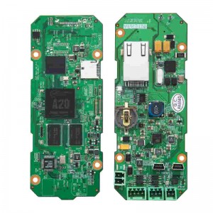
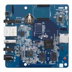
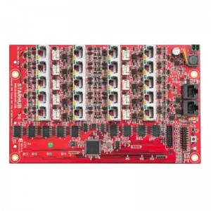
China New Design Mobile Communication PCB, Smartphone PCB
Products feature
● -HDI/Any-layer/mSAP
● -Fine line and multilayer manufacture capability
● -Advanced SMT and after assembly equipment
● -Exquisite craft
● -Isolated function test capability
● -Low loss material
● -5G Antenna Experience
Our Service
● Our Services: One-stop PCB and PCBA electronic manufacturing services
● PCB manufacturing service: Need Gerber file(CAM350 RS274X), PCB files (Protel 99, AD, Eagle), etc
● Components sourcing services: BOM list included detailed Part number and Designator
● PCB assembly services: The above files and Pick and Place files, assembly drawing
● Programming & Testing services: Program, instrouction and test method etc.
● Housing assembly services: 3D files, step or others
● Reverse engineering services: Samples and others
● Cable & wire assembly services: Specification & others
● Others services: Value-added services
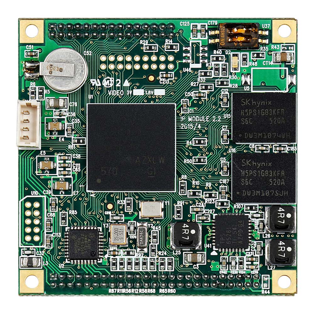
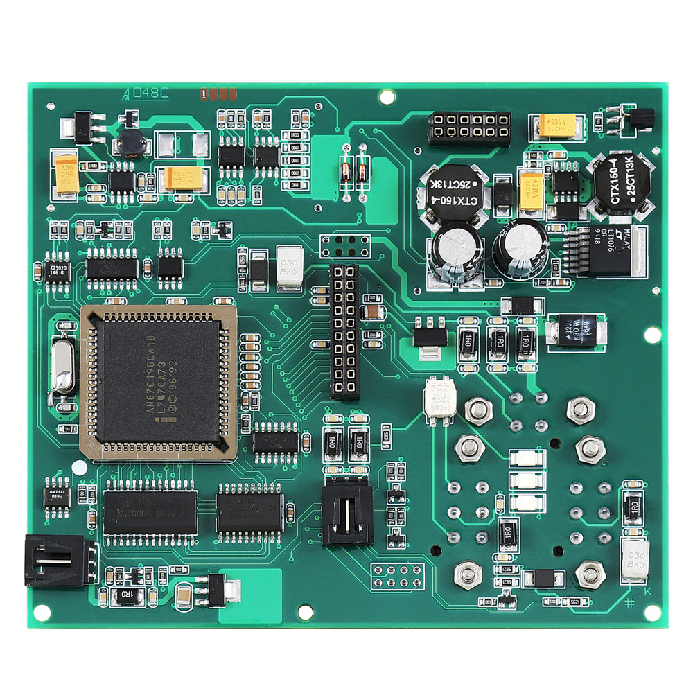
PCB Techinecal Capacity
| Layers | Mass production: 2~58 layers / Pilot run: 64 layers |
| Max. Thickness | Mass production: 394mil (10mm) / Pilot run: 17.5mm |
| Material | FR-4 (Standard FR4, Mid-Tg FR4,Hi-Tg FR4, Lead free assembly material) , Halogen-Free, Ceramic filled , Teflon, Polyimide, BT, PPO, PPE, Hybrid, Partial hybrid, etc. |
| Min. Width/Spacing | Inner layer: 3mil/3mil (HOZ), Outer layer: 4mil/4mil(1OZ) |
| Max. Copper Thickness | UL certificated: 6.0 OZ / Pilot run: 12OZ |
| Min. Hole Size | Mechanical drill: 8mil(0.2mm) Laser drill: 3mil(0.075mm) |
| Max. Panel Size | 1150mm × 560mm |
| Aspect Ratio | 18:1 |
| Surface Finish | HASL,Immersion Gold, Immersion Tin, OSP, ENIG + OSP, Immersion Silver, ENEPIG, Gold Finger |
| Special Process | Buried Hole, Blind Hole, Embedded Resistance, Embedded Capacity, Hybrid, Partial hybrid, Partial high density, Back drilling, and Resistance control |
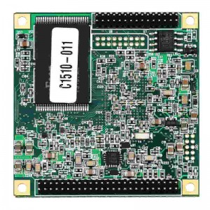
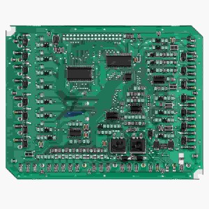
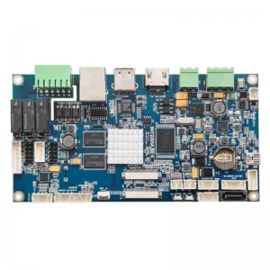
The mobile phone PCB is made of Shengyi S1000-2M material, which is produced with precision and professional technology. This choice ensures excellent performance and durability, allowing the board to withstand the demands of everyday use. In addition, the surface of the PCB is Gold-plated to ensure good electrical conductivity and signal transmission capabilities.
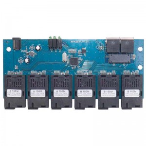
One of the outstanding features of this mobile communication PCB is the use of partial thick gold plating production technology. This technology provides enhanced corrosion protection, ensuring the longevity of the board. With this extra durability, manufacturers can confidently use this reliable PCB to assemble their smartphones or fiber optic communication devices.
In addition, China's newly designed mobile communication PCB demonstrates superior precision and attention to detail. It has a minimum bore diameter of 0.15 mm, enabling it to handle complex designs and assemblies. The minimum line width and line spacing of 120/ 85um ensure reliable electrical connection and reduce the risk of interference.
Specifically designed to meet the growing demands of fiber optic communication equipment products, this board is truly ideal. Its high-quality construction and advanced features make it a reliable and efficient solution for any communication device. Manufacturers can rely on this PCB to provide seamless connectivity , superior performance and excellent signal transmission.
In conclusion, China New Design Mobile Communication PCB offers cutting-edge technology and superior structure. With its Shengyi S1000-2M material, gold-plated surface and partly thick gold-plated production technology, this circuit board is at the front of the industry ry. Provide reliable, efficient and high-performance solutions for smartphone manufacturers and optical fiber communication equipment manufacturers. Choose China New Design Mobile Communication PCB for your next project and experience the difference in quality and performance.


