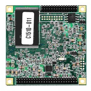
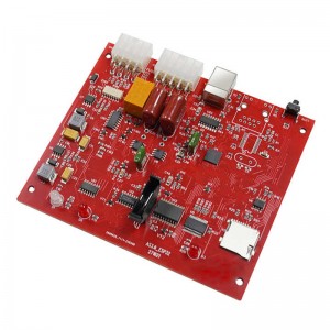
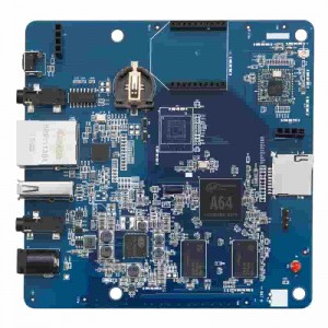
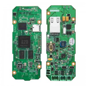
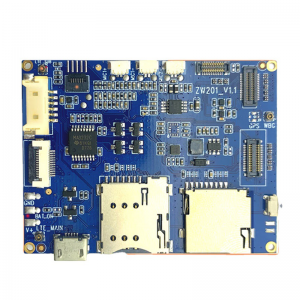
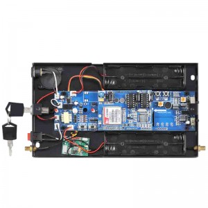
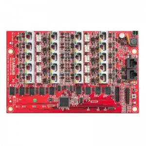
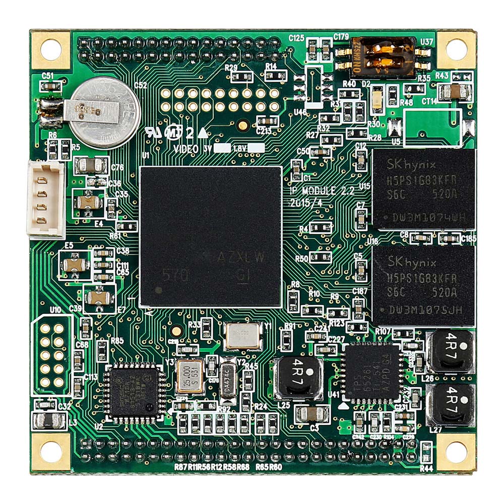
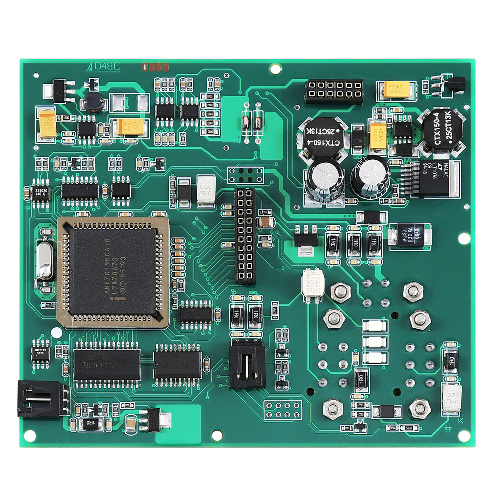
Mobile Phone PCBA board
Products feature
● -HDI/Any-layer/mSAP
● -Fine line and multilayer manufacture capability
● -Advanced SMT and after assembly equipment
● -Exquisite craft
● -Isolated function test capability
● -Low loss material
● -5G Antenna Experience
Our Service
● Our Services: One-stop PCB and PCBA electronic manufacturing services
● PCB manufacturing service: Need Gerber file(CAM350 RS274X), PCB files (Protel 99, AD, Eagle), etc
● Components sourcing services: BOM list included detailed Part number and Designator
● PCB assembly services: The above files and Pick and Place files, assembly drawing
● Programming & Testing services: Program, instrouction and test method etc.
● Housing assembly services: 3D files, step or others
● Reverse engineering services: Samples and others
● Cable & wire assembly services: Specification & others
● Others services: Value-added services
PCB Techinecal Capacity
| Layers | Mass production: 2~58 layers / Pilot run: 64 layers |
| Max. Thickness | Mass production: 394mil (10mm) / Pilot run: 17.5mm |
| Material | FR-4 (Standard FR4, Mid-Tg FR4,Hi-Tg FR4, Lead free assembly material) , Halogen-Free, Ceramic filled , Teflon, Polyimide, BT, PPO, PPE, Hybrid, Partial hybrid, etc. |
| Min. Width/Spacing | Inner layer: 3mil/3mil (HOZ), Outer layer: 4mil/4mil(1OZ) |
| Max. Copper Thickness | UL certificated: 6.0 OZ / Pilot run: 12OZ |
| Min. Hole Size | Mechanical drill: 8mil(0.2mm) Laser drill: 3mil(0.075mm) |
| Max. Panel Size | 1150mm × 560mm |
| Aspect Ratio | 18:1 |
| Surface Finish | HASL,Immersion Gold, Immersion Tin, OSP, ENIG + OSP, Immersion Silver, ENEPIG, Gold Finger |
| Special Process | Buried Hole, Blind Hole, Embedded Resistance, Embedded Capacity, Hybrid, Partial hybrid, Partial high density, Back drilling, and Resistance control |


