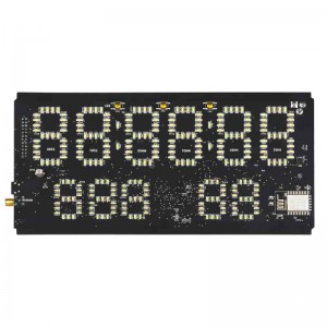
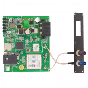
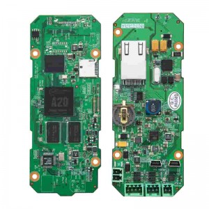
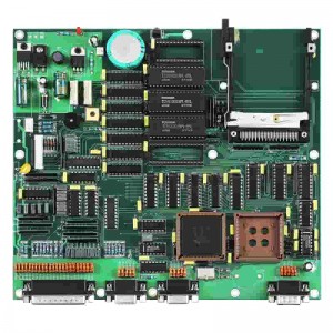
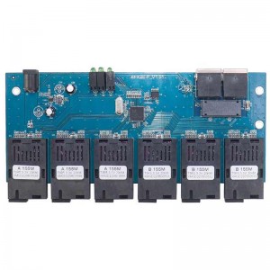
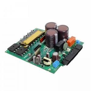
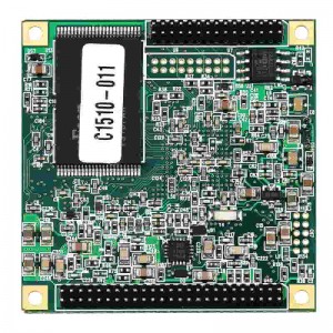
One stop electronic LED PCBA board manufacturer
Main Products
MPCB, a metal-based PCB, is comprised of a metal substrate (ie Aluminum, Copper or Stainless Steel ect.,), thermal dissipating dielectric and the copper circuit. Due to its superior heat dissipation, MPCBs are used for a wide array of applications. You can find them in power supplies, LED lighting or anywhere that heat is a major factor.
PCB structure characteristics
1.Circuit and pattern (Pattern): The circuit is used as a tool for conducting between components. In the design, a large copper surface will be designed as a grounding and power supply layer. Lines and drawings are made at the same time.
2.Dielectric layer (Dielectric): It is used to maintain the insulation between lines and layers, commonly known as the substrate.
3.Silkscreen (Legend/Marking/Silkscreen): This is a non-essential component. Its main function is to mark the name and position box of each part on the circuit board, which is convenient for maintenance and identification after assembly.
PCBA technical Capacity
| SMT | Position accuracy:20 um |
| Components size:0.4×0.2mm(01005) —130×79mm,Flip-CHIP,QFP,BGA,POP | |
| Max. component height::25mm | |
| Max. PCB size:680×500mm | |
| Min. PCB size:no limited | |
| PCB thickness:0.3 to 6mm | |
| PCB weight:3KG | |
| Wave-Solder | Max. PCB width:450mm |
| Min. PCB width: no limited | |
| Component height:Top 120mm/Bot 15mm | |
| Sweat-Solder | Metal type :part, whole, inlay, sidestep |
| Metal material:Copper , Aluminum | |
| Surface Finish:plating Au, plating sliver , plating Sn | |
| Air bladder rate:less than 20% | |
| Press-fit | Press range:0-50KN |
| Max. PCB size:800X600mm | |
| Testing | ICT,Probe flying,burn-in,function test,temperature cycling |
FAQ
Pls Confirm With Us The Modle You Need.And The Sample Fee Will Be Refunded In Bulk.
Sample Will Be Send Out Within 2days After Received Payment
Normally It Takes 5 Working Days After Received Payment.
100% QC Before Shipment.If There're Some Unexpected Problem Happan,Like Quality Problem
Normally It Takes 5 Working Days After Received Payment.


